- 您现在的位置:买卖IC网 > Sheet目录526 > SUD19N20-90-T4-E3 (Vishay Siliconix)MOSFET N-CH D-S 200V TO252
�� �
�
�SUD19N20-90�
�Vishay� Siliconix�
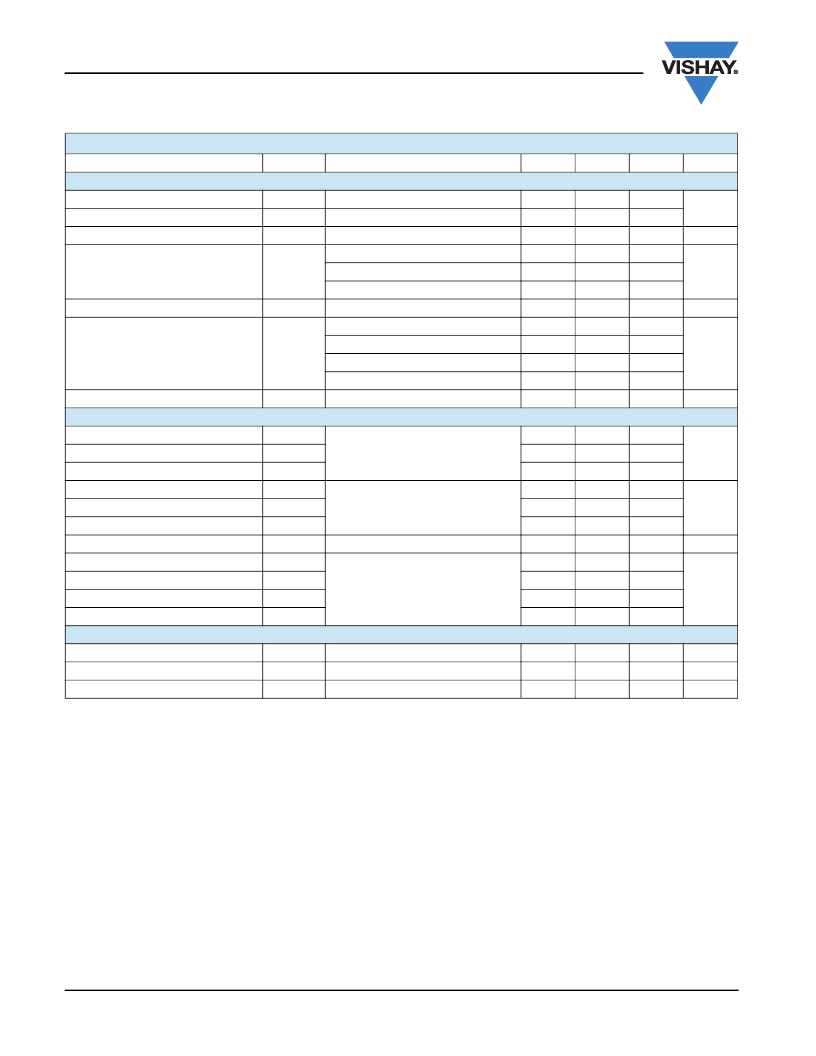
�SPECIFICATIONS� (T� J� =� 25� °C,� unless� otherwise� noted)�
�Parameter�
�Symbol�
�Test� Conditions�
�Min.�
�Typ.� a�
�Max.�
�Unit�
�Static�
�Drain-Source� Breakdown� Voltage�
�Gate� Threshold� Voltage�
�Gate-Body� Leakage�
�V� DS�
�V� GS(th)�
�I� GSS�
�V� GS� =� 0� V,� I� D� =� 250� μA�
�V� DS� =� V� GS� ,� I� D� =� 250� μA�
�V� DS� =� 0� V,� V� GS� =� ±� 20� V�
�200�
�2�
�4�
�±� 100�
�V�
�nA�
�V� DS� =� 200� V,� V� GS� =� 0� V�
�1�
�Zero� Gate� Voltage� Drain� Current�
�I� DSS�
�V� DS� =� 200� V,� V� GS� =� 0� V,� T� J� =� 125� °C�
�50�
�μA�
�V� DS� =� 200� V,� V� GS� =� 0� V,� T� J� =� 175� °C�
�250�
�On-State� Drain� Current� b�
�I� D(on)�
�V� DS� =� ?� 5� V,� V� GS� =� 10� V�
�V� GS� =� 10� V,� I� D� =� 5� A�
�40�
�0.075�
�0.090�
�A�
�Drain-Source� On-State� Resistance� b�
�R� DS(on)�
�V� GS� =� 10� V,� I� D� =� 5� A,� T� J� =� 125� °C�
�V� GS� =� 10� V,� I� D� =� 5� A,� T� J� =� 175� °C�
�V� GS� =� 6� V,� I� D� =� 5� A�
�0.082�
�0.190�
�0.260�
�0.105�
�?�
�Forward�
�Transconductance� b�
�g� fs�
�V� DS� =� 15� V,� I� D� =� 19� A�
�35�
�S�
�Dynamic� a�
�Input� Capacitance�
�C� iss�
�1800�
�Gate-Drain� Charge�
�Output� Capacitance�
�Reverse� Transfer� Capacitance�
�Total� Gate� Charge� c�
�Gate-Source� Charge� c�
�c�
�C� oss�
�C� rss�
�Q� g�
�Q� gs�
�Q� gd�
�V� GS� =� 0� V,� V� DS� =� 25� V,� F� =� 1� MHz�
�V� DS� =� 100� V,� V� GS� =� 10� V,� I� D� =� 19� A�
�180�
�80�
�34�
�8�
�12�
�51�
�pF�
�nC�
�Gate� Resistance�
�R� g�
�0.5�
�2.9�
�?�
�Turn-On� Delay�
�Time� c�
�t� d(on)�
�15�
�25�
�Rise� Time� c�
�Turn-Off� Delay� Time� c�
�Fall� Time� c�
�t� r�
�t� d(off)�
�t� f�
�V� DD� =� 100� V,� R� L� =� 5.2� ?�
�I� D� ?� 19� A,� V� GEN� =� 10� V,� R� g� =� 2.5� ?�
�50�
�30�
�60�
�75�
�45�
�90�
�ns�
�Source-Drain� Diode� Ratings� and� Characteristics� (T� C� =� 25� °C)�
�Pulsed� Current�
�I� SM�
�50�
�A�
�Diode� Forward� Voltage�
�b�
�V� SD�
�I� F� =� 19� A,� V� GS� =� 0� V�
�0.9�
�1.5�
�V�
�Source-Drain� Reverse� Recovery� Time�
�t� rr�
�I� F� =� 19� A,� dI/dt� =� 100� A/μs�
�180�
�250�
�ns�
�Notes:�
�a.� Guaranteed� by� design,� not� subject� to� production� testing.�
�b.� Pulse� test;� pulse� width� ?� 300� μs,� duty� cycle� ?� 2� %.�
�c.� Independent� of� operating� temperature.�
�Stresses� beyond� those� listed� under� “Absolute� Maximum� Ratings”� may� cause� permanent� damage� to� the� device.� These� are� stress� ratings� only,� and� functional� operation�
�of� the� device� at� these� or� any� other� conditions� beyond� those� indicated� in� the� operational� sections� of� the� specifications� is� not� implied.� Exposure� to� absolute� maximum�
�rating� conditions� for� extended� periods� may� affect� device� reliability.�
�www.vishay.com�
�2�
�Document� Number:� 71767�
�S10-2245-Rev.� E,� 04-Oct-10�
�发布紧急采购,3分钟左右您将得到回复。
相关PDF资料
SUD19P06-60L-E3
MOSFET P-CH D-S 60V TO252
SUD23N06-31-T4-GE3
MOSFET N-CH D-S 60V TO252
SUD23N06-31L-E3
MOSFET N-CH D-S 60V TO252
SUD25N15-52-T4-E3
MOSFET N-CH D-S 150V TO252
SUD35N05-26L-E3
MOSFET N-CH D-S 55V TO252
SUD40N02-08-E3
MOSFET N-CH D-S 20V TO252
SUD50N02-09P-E3
MOSFET N-CH D-S 20V DPAK
SUD50N03-06P-E3
MOSFET N-CH D-S 30V TO252
相关代理商/技术参数
SUD19P06-60
制造商:VISHAY 制造商全称:Vishay Siliconix 功能描述:P-Channel 60-V (D-S) MOSFET
SUD19P06-60-E3
功能描述:MOSFET 60V 19A 38.5W RoHS:否 制造商:STMicroelectronics 晶体管极性:N-Channel 汲极/源极击穿电压:650 V 闸/源击穿电压:25 V 漏极连续电流:130 A 电阻汲极/源极 RDS(导通):0.014 Ohms 配置:Single 最大工作温度: 安装风格:Through Hole 封装 / 箱体:Max247 封装:Tube
SUD19P06-60-GE3
功能描述:MOSFET 60V 19A 38.5W 60mohm @ 10V RoHS:否 制造商:STMicroelectronics 晶体管极性:N-Channel 汲极/源极击穿电压:650 V 闸/源击穿电压:25 V 漏极连续电流:130 A 电阻汲极/源极 RDS(导通):0.014 Ohms 配置:Single 最大工作温度: 安装风格:Through Hole 封装 / 箱体:Max247 封装:Tube
SUD19P06-60-GE3
制造商:Vishay Siliconix 功能描述:P CHANNEL MOSFET -60V 19A TO-252
SUD19P06-60L
制造商:VAISH 制造商全称:VAISH 功能描述:P-Channel 60-V (D-S) 175C MOSFET
SUD19P06-60L-E3
功能描述:MOSFET 60V 19A 46W 60mohm @ 10V RoHS:否 制造商:STMicroelectronics 晶体管极性:N-Channel 汲极/源极击穿电压:650 V 闸/源击穿电压:25 V 漏极连续电流:130 A 电阻汲极/源极 RDS(导通):0.014 Ohms 配置:Single 最大工作温度: 安装风格:Through Hole 封装 / 箱体:Max247 封装:Tube
SUD20N10-66L-GE3
制造商:Vishay Semiconductors 功能描述:N-CH MOSFET DPAK (TO-252) 100V 66MOHM @ 10V - Tape and Reel 制造商:Vishay Intertechnologies 功能描述:N-Ch MOSFET DPak (TO-252) 100V 66mohm @ 10V
SUD23N06
制造商:SHENZHENFREESCALE 制造商全称:ShenZhen FreesCale Electronics. Co., Ltd 功能描述:N-Channel 60 V (D-S) 175 ?°C MOSFET